
The electronics that power our smartphones, computers, and even our cars are often made in spaces cleaner than a hospital operating room. The smaller and more intricate the parts, the more sensitive they are to damage by tiny particles.
According to Moore’s Law, the number of transistors on an integrated circuit will double every two years, which means they will become sensitive to smaller and smaller particles. This makes cleanrooms more important than ever.
The semiconductor industry in particular relies heavily on cleanrooms to produce the microchips and integrated circuits that power many modern technologies. In this article, we’ll explore what semiconductor cleanrooms are, their classifications, design features, and more.
What Are Semiconductor Cleanrooms?
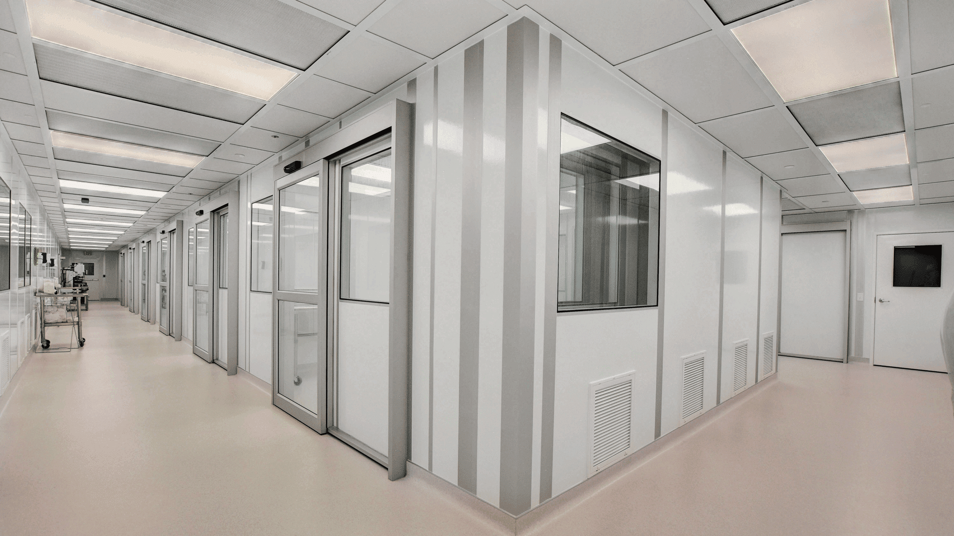
Semiconductor cleanrooms are controlled environments where airborne particles and several conditions, such as temperature, humidity, and static electricity, are carefully managed. Such spaces are designed to prevent contamination of semiconductors during many stages of manufacturing, including photolithography, wafer fabrication, and even packaging and assembly.
Why Semiconductors Require Cleanrooms

Semiconductor manufacturing is composed of processes that are extremely precise, with circuit features measured in nanometers. At this scale, even microscopic particles can cause big problems that may result in the complete loss of product.
Stages of production that are particularly at risk are photolithography, etching, and deposition. It only takes a single particle to obstruct the pathway of a circuit. And because wafers pass through many processes, contamination at any point can reduce destroy batches, and in turn lead to lower yields.
As a result, the stability of the environment is of prime importance. Even minor fluctuations in conditions like temperature or humidity can lead to problems like layer inconsistencies or electrostatic discharge (ESD), which damages parts.
Electronics also need to be reliable, especially for applications like autombiles, medical devices, and aerospace, where errors can become dangerous. Since semiconductors have become the backbone of many modern products, cleanrooms have become essential to creating tightly controlled environments.
Applications of Semiconductor Cleanrooms
Semiconductor cleanrooms are used in many parts of the manufacturing process. Some common applications include:
- Wafer fabrication
- Photolithography
- Etching
- Deposition
- Metrology, inspection, and testing
- Assembly & packaging
- R&D
ISO Classifications of Semiconductor Cleanrooms

Cleanrooms, within the ISO 14644-1 framework, are classified based on the number of particles per cubic meter of air. The standard defines cleanroom classes from ISO Class 1 to ISO Class 9, with ISO Class 1 being the strictest, allowing the fewest particles, and ISO Class 9 permitting the most.
For most processes, semiconductor cleanrooms require compliance with ISO Class 4 to ISO Class 6; however, they may at some times be more strict, depending on the application. Stages such as photolithography and wafer fabrication, for example, often require more demanding cleanrooms.
Packaging and assembly, on the other hand, are still required to be clean, but much less so, which is why such operations are often housed in ISO Class 7 or ISO Class 8 cleanrooms.
What are the Design Features of Semiconductor Cleanrooms?
Several design aspects of these cleanrooms are important for successful operations. Here are some of the most significant:
- Air Filtration: Semiconductors use high-efficiency particulate air (HEPA) filters and ultra-low penetration air (ULPA) filters to effectively remove tiny particles from the air. These filters can capture particles as small as 0.3 and 0.12 micrometers, respectively.
- Humidity Control: Controlling humidity levels is another important variable in semiconductor cleanrooms, especially because of its relationship to static electricity. By keeping humidity levels above 30%, these spaces reduce the risk of electrostatic discharge, which can damage semiconductors.
- Electrostatic Discharge (ESD) Control: A corollary of the above. Semiconductor often need to have static-dissipative flooring and grounded surfaces (in addition to controlled humidity) to reduce the possibility electrostatic discharge.
- Temperature Control: Maintaining stable temperatures is also necessary, both to prevent damage to semiconductor materials and to keep personnel safe and comfortable.
- Airflow: Unidirectional airflow, also known as laminar airflow, is another important design feature often found in semiconductor cleanrooms. It’s just what it sounds like: airflow that moves in one direction, typically downward or horizontally, to sweep away contaminants.
- Monitoring Systems: Monitoring is another central aspect in protecting semiconductor processes. Particle counters and environmental control systems track air quality and detect contamination. They provide real-time data, so any deviation in conditions can quickly be addressed.
The Bottom Line
When even a tiny particle can ruin or damage electrical parts, cleanrooms become indispensable in the manufacturing process. The recent surge in semiconductor demand has made cleanrooms essential for product reliability. As semiconductors make their way into more and more products, the industry will continue to rely on cleanrooms. And as parts shrink, cleanroom technology will need to innovate to meet the growing need for both precision and cleanliness.
FAQs About Semiconductor Cleanrooms
What’s the difference between semiconductor cleanrooms and other kinds of cleanrooms?
Semiconductor cleanrooms are in many if not most cases far stricter. They place tighter limits on particles, have higher air-change rates, and need to prevent electrostatic discharge and other issues that can affect products. Whereas in pharmaceutical cleanrooms the emphasis is more on viable particles, with semiconductors, the danger is with any particles whatsover.
What particle sizes are most important to avoid in semiconductor manufacturing?
Different processes will require different ISO classifications, and as a result, the particle sizes that cause trouble will be different. However, speaking generally, we can say that particles smaller than 0.5 micrometers are particularly important to avoid, as these can especially interfere with features at nanoscale.
Are modular cleanrooms an option for semiconductor applications?
Modular cleanroom are used commonly in semiconductor manufacturing. This is because of their flexibility (ability to be scaled later), as well as the ability to meet requirements at lower upfront costs.